TDA7294 ST 100V – 100W DMOS Audio Amplifier with Mute/ST-BY Data Sheet
Download PDF datasheet for STMicroelectronics TDA7294 100V 100W DMOS Audio Amplifier with MUTE/ST-BY (EN) 16 pages 1996 zip
Description
This PDF datasheet is for the ST TDA7294 Audio Amplifier.
About the Item
ST TDA7294 100V 100W DMOS Audio Amplifier with MUTE/ST-BY
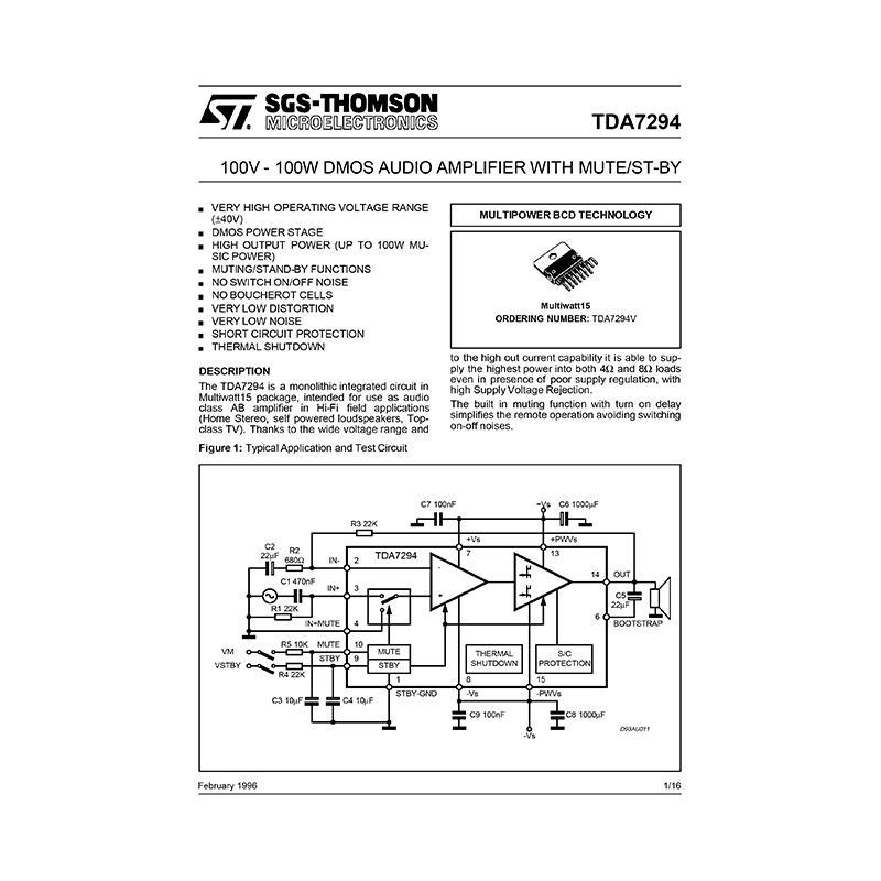
– VERY HIGH OPERATING VOLTAGE RANGE (+/-40V)
– DMOS POWER STAGE
– HIGH OUTPUT POWER (UP TO 100W MUSIC POWER)
– MUTING/STAND-BY FUNCTIONS
– NO SWITCH ON/OFF NOISE
– NO BOUCHEROT CELLS
– VERY LOW DISTORTION
– VERY LOW NOISE
– SHORT CIRCUIT PROTECTION
– THERMAL SHUTDOWN
The TDA7294 is a monolithic integrated circuit in Multiwatt15 package, intended for use as audio class AB amplifier in Hi-Fi field applications (Home Stereo, self powered loudspeakers, Top-class TV). Thanks to the wide voltage range and to the high out current capability it is able to supply the highest power into both 4 Ohm and 8 Ohm loads even in presence of poor supply regulation, with high Supply Voltage Rejection.
The built in muting function with turn on delay simplifies the remote operation avoiding switching on-off noises.
(PDF) DATASHEET (ENGLISH)
SUMMARY OF CONTENTS
– Figure 1: Typical Application and Test Circuit
– TDA7294 PIN CONNECTION (PINOUT)
– BLOCK DIAGRAM
– ABSOLUTE MAXIMUM RATINGS
– THERMAL DATA
– ELECTRICAL CHARACTERISTICS
– Figure 2: P.C.B. and components layout of the circuit of figure 1. (1:1 scale)
– APPLICATION SUGGESTIONS
– TYPICAL CHARACTERISTICS:
– Figure 3: Output Power vs. Supply Voltage
– Figure 4: Distortion vs. Output Power
– Figure 5: Output Power vs. Supply Voltage
– Figure 6: Distortion vs. Output Power
– Figure 7: Distortion vs. Frequency
– Figure 8: Distortion vs. Frequency
– Figure 9: Quiescent Current vs. Supply Voltage
– Figure 10: Supply Voltage Rejection vs. Frequency
– Figure 11: Mute Attenuation vs. V pin 10
– Figure 12: St-by Attenuation vs. V pin 9
– Figure 13: Power Dissipation vs. Output Power 4 Ohms
– Figure 14: Power Dissipation vs. Output Power 8 Ohms
– Figure 15: Principle Schematic of a DMOS unity-gain buffer.
– Figure 16: Turn ON/OFF Suggested Sequence
– Figure 17: Single Signal ST-BY/MUTE Control Circuit
– Figure 18: High Efficiency Application Circuit
– Figure 19: P.C.B. and Components Layout of the Circuit of figure 18 (1:1 scale)
– Figure 20: Power Dissipation vs. Output Power
– Figure 21: Distortion vs. Output Power
– Figure 22: Distortion vs. Output Power
– Figure 23: Power Dissipation vs. Output Power
– Figure 24: Power Dissipation vs. Output Power
– Figure 25: Bridge Application Circuit
– Figure 26: Frequency Response of the Bridge Application
– Figure 27: Distortion vs. Output Power
– Figure 28: Distortion vs. Output Power
– MULTIWATT15 PACKAGE MECHANICAL DATA
Why download the Datasheet?
This datasheet provides all the information from ST about the TDA7294 Audio Amplifier, as detailed in the table of contents. Reading it completely will address most questions you might have. You can download and save it for offline use, including viewing it on your device or printing it for your convenience if you prefer a paper version.
How to download the Datasheet?
Download it by clicking the button below
Helped you out?
Glad to hear that. It would be awesome if you could . . .


