TDA7293 ST 120V – 100W DMOS Audio Amplifier with Mute/ST-BY Data Sheet
Download PDF datasheet for STMicroelectronics TDA7293 120V 100W DMOS Audio Amplifier with MUTE/ST-BY (EN) 13 pages 1999 zip
Description
This PDF datasheet is for the ST TDA7293 Audio Amplifier.
About the Item
ST TDA7293 120V 100W DMOS Audio Amplifier with MUTE/ST-BY
– VERY HIGH OPERATING VOLTAGE RANGE (+/-50V)
– DMOS POWER STAGE
– HIGH OUTPUT POWER (100W @ THD = 10%, RL = 8Ohms, VS = +/-40V)
– MUTING/STAND-BY FUNCTIONS
– NO SWITCH ON/OFF NOISE
– VERY LOW DISTORTION
– VERY LOW NOISE
– SHORT CIRCUIT PROTECTION
– THERMAL SHUTDOWN
– CLIP DETECTOR
– MODULARITY (MORE DEVICES CAN BE EASILY CONNECTED IN PARALLEL TO DRIVE VERY LOW IMPEDANCES)
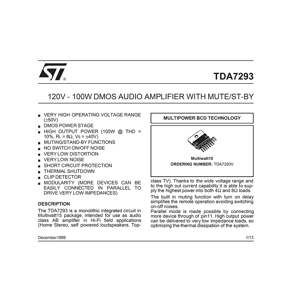
The TDA7293 is a monolithic integrated circuit in Multiwatt15 package, intended for use as audio class AB amplifier in Hi-Fi field applications (Home Stereo, self powered loudspeakers, Top-class TV). Thanks to the wide voltage range and to the high out current capability it is able to supply the highest power into both 4 Ohm and 8 Ohm loads.
The built in muting function with turn on delay simplifies the remote operation avoiding switching on-off noises.
Parallel mode is made possible by connecting more device through of pin11. High output power can be delivered to very low impedance loads, so optimizing the thermal dissipation of the system.
(PDF) DATASHEET (ENGLISH)
SUMMARY OF CONTENTS
– Figure 1: Typical Application and Test Circuit
– TDA7293 PIN CONNECTION (PINOUT)
– QUICK REFERENCE DATA
– ABSOLUTE MAXIMUM RATINGS
– THERMAL DATA
– ELECTRICAL CHARACTERISTICS
– Figure 2: Typical Application P.C. Board and Component Layout (scale 1:1)
– APPLICATION SUGGESTIONS
– Slave function: pin 4 (Ref to pin 8 -VS)
– Figure 3: Principle Schematic of a DMOS unity-gain buffer.
– Figure 4: Turn ON/OFF Suggested Sequence
– Figure 5: Single Signal ST-BY/MUTE Control Circuit
– Figure 6: High Efficiency Application Circuit
– Figure 6a: PCB and Component Layout of the fig. 6
– Figure 6b: PCB – Solder Side of the fig. 6.
– Figure 7: Modular Application Circuit
– Figure 8a: Modular Application P.C. Board and Component Layout (scale 1:1) (Component SIDE)
– Figure 8b: Modular Application P.C. Board and Component Layout (scale 1:1) (Solder SIDE)
– OUTLINE AND MECHANICAL DATA
Why download the Datasheet?
This datasheet provides all the information from ST about the TDA7293 Audio Amplifier, as detailed in the table of contents. Reading it completely will address most questions you might have. You can download and save it for offline use, including viewing it on your device or printing it for your convenience if you prefer a paper version.
How to download the Datasheet?
Download it by clicking the button below
Helped you out?
Glad to hear that. It would be awesome if you could . . .


