TDA2822 ST Dual Power Amplifier Data Sheet
Download PDF datasheet for SGS-Thomson Microelectronics / ST TDA2822 Dual Power Amplifier Integrated Circuit (EN) 11 pages 1995 zip
Description
This PDF data sheet is for the SGS-Thomson / ST TDA2822 power amplifier.
About the Item
SGS-Thomson Microelectronics TDA2822 Dual Power Amplifier Integrated Circuit
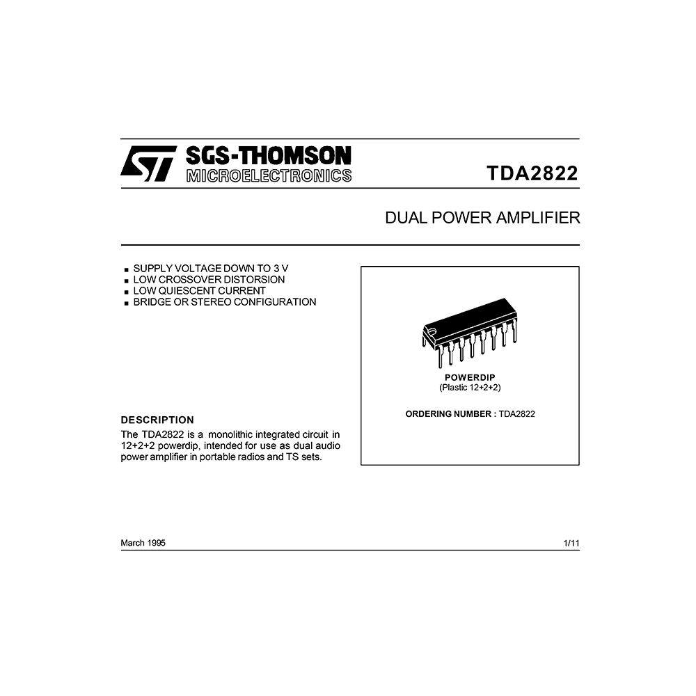
The TDA2822 is a monolithic integrated circuit in 12+2+2 powerdip, intended for use as dual audio power amplifier in portable radios and TV sets.
Document(s) available
(PDF) DATASHEET
Available languages
ENGLISH (EN)
SUMMARY OF CONTENTS
– Ordering Number
– Typical Application Circuit (Stereo)
– Pin Connection. TDA2822 pinout.
– Schematic Diagram
– Absolute Maximum Ratings. Supply Voltage. Output Peak Current. Total Power Dissipation. Storage and Junction Temperature.
– Thermal Data
– Electrical Characteristics
Figure 1: Test Circuit (stereo).
Figure 2: P.C. Board and Components Layout of the Circuit of Figure 1 (1:1 scale)
Figure 3: Test Circuit (bridge)
Figure 4: P.C. Board and Components Layout of the Circuit of Figure 3 (1:1 scale)
Figure 5: Output Power vs. Supply Voltage (Stereo)
Figure 6: Output Power vs. Supply Voltage (Bridge)
Figure 7: Distorsion vs. Output Power (Bridge)
Figure 8: Distorsion vs. Output Power (Bridge)
Figure 9: Supply Voltage Rejection vs. Frequency
Figure 10: Quiescent Current vs. Supply Voltage
Figure 11: Total Power Dissipation vs. Output Power (Stereo)
Figure 12: Total Power Dissipation vs. Output Power (Bridge)
Figure 13: Total Power Dissipation vs. Output Power (Bridge)
Figure 14: Application Circuit for Portable Radios
– Mounting Instruction
Figure 15: Example of P.C. Board Copper Area which is used as Heatsink.
Figure 16: External Heatsink Mounting Example.
Figure 6 : Maximum Dissipable Power and
– Junction to Ambient Thermal Resistance vs. Side “delta”.
Figure 7 : Maximum Allowable Power Dissipation vs. Ambient Temperature.
– Powerdip 16 Package Mechanical Data
Why download the Datasheet?
This datasheet provides all the information from SGS-THOMSON MICROELECTRONICS / ST about the TDA2822 power amplifier, as detailed in the table of contents. Reading it completely will address most questions you might have. You can download and save it for offline use, including viewing it on your device or printing it for your convenience if you prefer a paper version.
How to download the Datasheet?
Download it by clicking the button below
Helped you out?
Glad to hear that. It would be awesome if you could . . .


