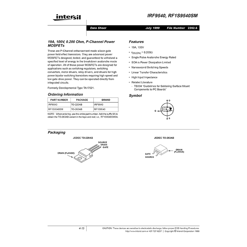
RF1S9540SM Intersil 19A 100V P-Channel Power MOSFET Data Sheet
Download PDF datasheet for Intersil RF1S9540SM P-Channel 19A 100V 0.200 Ohm TO-263AB Power MOSFET (EN) 7 pages 2282.6 1999 zip
Description
This PDF datasheet is for the Intersil RF1S9540SM Power MOSFET
About the Item
Intersil RF1S9540SM 19A 100V 0.200 Ohm P-Channel TO-263AB Power MOSFET
These are P-Channel enhancement mode silicon gate power field effect transistors. They are advanced power MOSFETs designed, tested, and guaranteed to withstand a specified level of energy in the breakdown avalanche mode of operation. All of these power MOSFETs are designed for applications such as switching regulators, switching convertors, motor drivers, relay drivers, and drivers for high power bipolar switching transistors requiring high speed and low gate drive power. They can be operated directly from integrated circuits.
Formerly Developmental Type TA17521.
FEATURES
– 19A, 100V
– rDS(ON) = 0.200 Ohm
– Single Pulse Avalanche Energy Rated
– SOA is Power Dissipation Limited
– Nanosecond Switching Speeds
– Linear Transfer Characteristics
– High Input Impedance
– Related Literature
– TB334 “Guidelines for Soldering Surface Mount Components to PC Boards”
Document(s) available
(PDF) DATASHEET
Available languages
ENGLISH (EN)
SUMMARY OF CONTENTS
– ABSOLUTE MAXIMUM RATINGS
– RF1S9540SM PINOUT
– INTERNAL SCHEMATIC DIAGRAM
– ELECTRICAL SPECIFICATIONS
– SOURCE TO DRAIN DIODE SPECIFICATIONS
– TYPICAL PERFORMANCE CURVES
FIGURE 1. NORMALIZED POWER DISSIPATION vs CASE TEMPERATURE
FIGURE 2. MAXIMUM CONTINUOUS DRAIN CURRENT vs CASE TEMPERATURE
FIGURE 3. NORMALIZED MAXIMUM TRANSIENT THERMAL IMPEDANCE
FIGURE 4. FORWARD BIAS SAFE OPERATING AREA
FIGURE 5. OUTPUT CHARACTERISTICS
FIGURE 6. SATURATION CHARACTERISTICS
FIGURE 7. TRANSFER CHARACTERISTICS
FIGURE 8. DRAIN TO SOURCE ON RESISTANCE vs GATE VOLTAGE AND DRAIN CURRENT
FIGURE 9. NORMALIZED DRAIN TO SOURCE ON RESISTANCE vs JUNCTION TEMPERATURE
FIGURE 10. NORMALIZED DRAIN TO SOURCE BREAKDOWN VOLTAGE vs JUNCTION TEMPERATURE
FIGURE 11. CAPACITANCE vs DRAIN TO SOURCE VOLTAGE
FIGURE 12. TRANSCONDUCTANCE vs DRAIN CURRENT
FIGURE 13. SOURCE TO DRAIN DIODE VOLTAGE
FIGURE 14. GATE TO SOURCE VOLTAGE vs GATE CHARGE
TEST CIRCUITS AND WAVEFORMS:
FIGURE 15. UNCLAMPED ENERGY TEST CIRCUIT
FIGURE 16. UNCLAMPED ENERGY WAVEFORMS
FIGURE 17. SWITCHING TIME TEST CIRCUIT
FIGURE 18. RESISTIVE SWITCHING WAVEFORMS
FIGURE 19. GATE CHARGE TEST CIRCUIT
FIGURE 20. GATE CHARGE WAVEFORMS
Why download the Datasheet?
This datasheet provides all the information from Intersil RF1S9540SM Power MOSFET, as detailed in the table of contents. Reading it completely will address most questions you might have. You can download and save it for offline use, including viewing it on your device or printing it for your convenience if you prefer a paper version.
How to download the Datasheet?
Download it by clicking the button below
Helped you out?
Glad to hear that. It would be awesome if you could . . .


