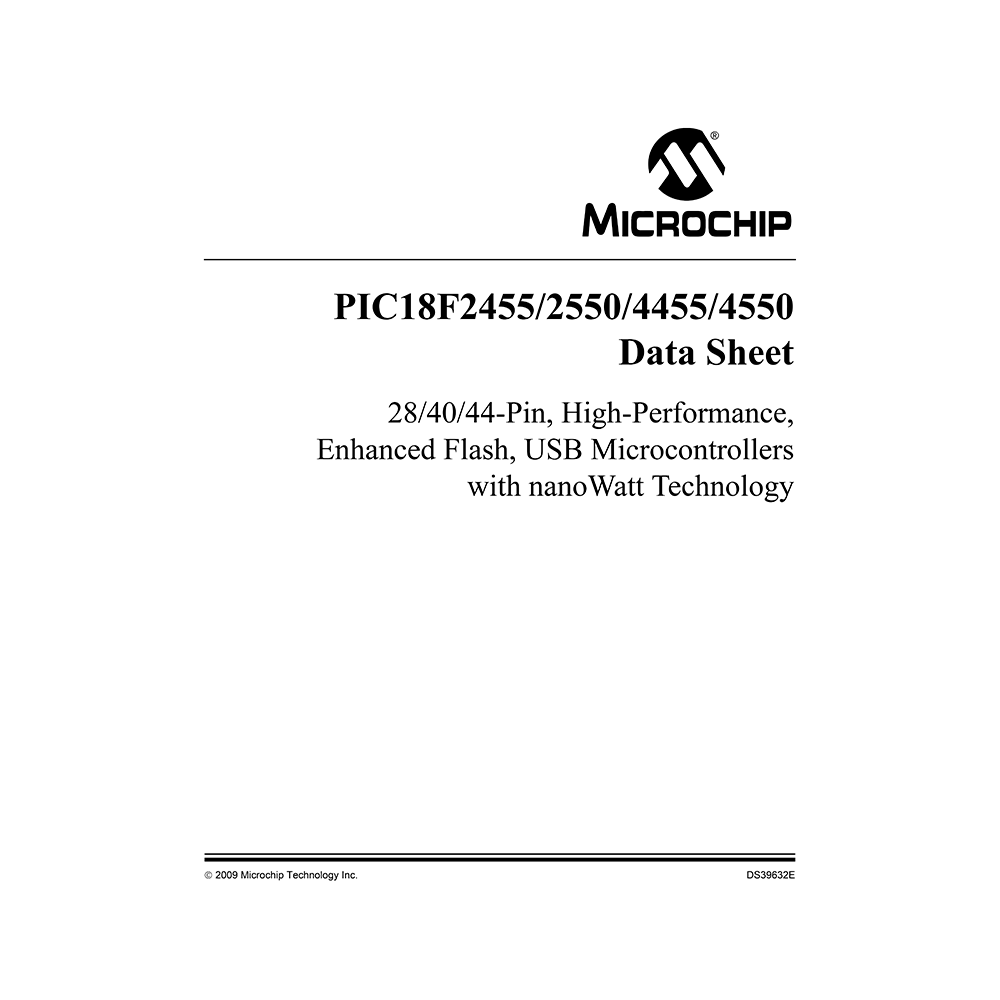
PIC18F4550 Microchip 40/44-Pin High-Performance Enhanced Flash USB Microcontroller Data Sheet
Download PDF datasheet for Microchip Technology PIC18F4550 Microcontroller with nanoWatt technology (EN) 438 pages DS39632E 2009 zip
Description
This PDF datasheet is for the Microchip PIC18F4550 Microcontroller.
About the Item
Microchip PIC18F4550 High-Performance Enhanced Flash USB Microcontroller with nanoWatt Technology
This family of devices offers the advantages of all PIC18 microcontrollers – namely, high computational performance at an economical price – with the addition of high-endurance, Enhanced Flash program memory.
In addition to these features, the PIC18F4550 family introduces design enhancements that make these microcontrollers a logical choice for many high-performance, power sensitive applications.
(PDF) DATASHEET (ENGLISH)
SUMMARY OF CONTENTS
– Pin Diagrams
1.0 DEVICE OVERVIEW. New Core Features. Other Special Features. Details on Individual Family Members. Block diagram. Pinout I/O descriptions.
2.0 OSCILLATOR CONFIGURATIONS. Overview. Oscillator Types. Clock diagram. Oscillator Settings for USB. Clock Sources and Oscillator Switching. Effects of Power-Managed Modes on the Various Clock Sources. Power-up Delays.
3.0 POWER-MANAGED MODES. Selecting Power-Managed Modes. Run Modes. Sleep Mode. Idle Modes. Exiting Idle and Sleep Modes.
4.0 RESET. RCON Register. Master Clear Reset (MCLR). Power-on Reset (POR). Brown-out Reset (BOR). Device Reset Timers. Reset State of Registers.
5.0 MEMORY ORGANIZATION. Program Memory Organization. PIC18 Instruction Cycle. Data Memory Organization. Data Addressing Modes. Program Memory and the Extended Instruction Set. Data Memory and the Extended Instruction Set.
6.0 FLASH PROGRAM MEMORY. Table Reads and Table Writes. Control Registers. Reading the Flash Program Memory. Erasing Flash Program Memory. Writing to Flash Program Memory. Flash Program Operation During Code Protection.
7.0 DATA EEPROM MEMORY. EECON1 and EECON2 Registers. Reading the Data EEPROM Memory. Writing to the Data EEPROM Memory. Write Verify. Operation During Code-Protect. Protection Against Spurious Write. Using the Data EEPROM.
8.0 8 x 8 HARDWARE MULTIPLIER. Introduction. Operation.
9.0 INTERRUPTS. USB Interrupts. INTCON Registers. PIR Registers. PIE Registers. IPR Registers. RCON Register. INTx Pin Interrupts. TMR0 Interrupt. PORTB Interrupt-on-Change. Context Saving During Interrupts.
10.0 I/O PORTS. PORTA, TRISA and LATA Registers. PORTB, TRISB and LATB Registers. PORTC, TRISC and LATC Registers. PORTD, TRISD and LATD Registers. PORTE, TRISE and LATE Registers.
11.0 Timer0 MODULE. Timer0 Operation. Timer0 Reads and Writes in 16-Bit Mode. Prescaler. Timer0 Interrupt.
12.0 Timer1 MODULE. Timer1 Operation. Timer1 16-Bit Read/Write Mode. Timer1 Oscillator. Timer1 Interrupt. Resetting Timer1 Using the CCP Special Event Trigger. Using Timer1 as a Real-Time Clock. Considerations in Asynchronous Counter Mode.
13.0 Timer2 MODULE. Timer2 Operation. Timer2 Interrupt. TMR2 Output.
14.0 Timer3 MODULE. Timer3 Operation. Timer3 16-Bit Read/Write Mode. Using the Timer1 Oscillator as the Timer3 Clock Source. Timer3 Interrupt. Resetting Timer3 Using the CCP Special Event Trigger.
15.0 Capture/Compare/PWM (CCP) MODULES. CCP Module Configuration. Capture Mode. Compare Mode. PWM Mode.
16.0 Enhanced Capture/Compare/PWM (ECCP) MODULE. ECCP Outputs and Configuration. Capture and Compare Modes. Standard PWM Mode. Enhanced PWM Mode.
17.0 UNIVERSAL SERIAL BUS (USB). Overview of the USB Peripheral. USB Status and Control. USB RAM. Buffer Descriptors and the Buffer Descriptor Table. USB Interrupts. USB Power Modes. Streaming Parallel Port. Oscillator. Overview of USB.
18.0 STREAMING PARALLEL PORT. SPP Configuration. Setup for USB Control. Setup for Microcontroller Control.
19.0 MASTER SYNCHRONOUS SERIAL PORT (MSSP) MODULE. Master SSP (MSSP) Module Overview. Control Registers. SPI Mode. I2C Mode.
20.0 ENHANCED UNIVERSAL SYNCHRONOUS ASYNCHRONOUS RECEIVER TRANSMITTER (EUSART). Baud Rate Generator (BRG). EUSART Asynchronous Mode. EUSART Synchronous Master Mode. EUSART Synchronous Slave Mode.
21.0 10-Bit Analog-to-Digital Converter (A/D) MODULE. A/D Acquisition Requirements. Selecting and Configuring Acquisition Time. Selecting the A/D Conversion Clock. Operation in Power-Managed Modes. Configuring Analog Port Pins. A/D Conversions. Discharge. Use of the CCP2 Trigger.
22.0 COMPARATOR MODULE. Comparator Configuration. Comparator Operation. Comparator Reference. Comparator Response Time. Comparator Outputs. Comparator Interrupts. Comparator Operation During Sleep. Effects of a Reset. Analog Input Connection Considerations.
23.0 COMPARATOR VOLTAGE REFERENCE MODULE. Configuring the Comparator Voltage Reference. Voltage Reference Accuracy/Error. Operation During Sleep. Effects of a Reset. Connection Considerations.
24.0 High/Low-Voltage Detect (HLVD). Operation. HLVD Setup. Current Consumption. HLVD Start-up Time. Applications. Operation During Sleep. Effects of a Reset.
25.0 SPECIAL FEATURES of the CPU. Configuration Bits. Watchdog Timer (WDT). Two-Speed Start-up. Fail-Safe Clock Monitor. Program Verification and Code Protection. ID Locations. In-Circuit Serial Programming. In-Circuit Debugger. Special ICPORT Features (44-Pin TQFP Package Only). Single-Supply ICSP Programming.
26.0 INSTRUCTION SET SUMMARY. Standard Instruction Set. Extended Instruction Set.
27.0 DEVELOPMENT SUPPORT. MPLAB Integrated Development Environment Software. MPASM Assembler. MPLAB C18 and MPLAB C30 C Compilers. MPLINK Object Linker/MPLIB Object Librarian. MPLAB ASM30 Assembler, Linker and Librarian. MPLAB SIM Software Simulator. MPLAB ICE 2000 High-Performance In-Circuit Emulator. MPLAB REAL ICE In-Circuit Emulator System. MPLAB ICD 2 In-Circuit Debugger. MPLAB PM3 Device Programmer. PICSTART Plus Development Programmer. PICkit 2 Development Programmer. Demonstration, Development and Evaluation Boards.
28.0 ELECTRICAL CHARACTERISTICS. Absolute Maximum Ratings. DC Characteristics. AC (Timing) Characteristics.
29.0 DC and AC Characteristics GRAPHS and TABLES
30.0 PACKAGING INFORMATION
Appendix A: Revision History
Appendix B: Device Differences
Appendix C: Conversion Considerations
Appendix D: Migration From Baseline to Enhanced Devices
Appendix E: Migration From Mid-Range to Enhanced Devices
Appendix F: Migration From High-End to Enhanced Devices
– PIC18F4550 Product Identification System
Why Download the Datasheet?
This datasheet provides all the information from Microchip Technology about the PIC18F4550 Microcontroller, as detailed in the table of contents. Reading it completely will address most questions you might have. You can download and save it for offline use, including viewing it on your device or printing it for your convenience if you prefer a paper version.
How to Download the Datasheet?
Download it by clicking the button below
Helped you out?
Glad to hear that. It would be awesome if you could . . .


