LM321 TI Single Operational Amplifier Data Sheet
Download PDF datasheet for Texas Instruments LM321 Low Power Single Operational Amplifier (EN) 23 pages SNOS935C Rev.C 2014 zip
Description
This PDF datasheet is for the Texas Instruments LM321 operational amplifier.
About the Item
Texas Instruments LM321 Low Power Single Operational Amplifier
The LM321 brings performance and economy to low power systems. With a high unity gain frequency and a specified 0.4-V/us slew rate, the quiescent current is only 430-uA/amplifier (5 V). The input common mode range includes ground and therefore the device is able to operate in single supply applications as well as in dual supply applications. It is also capable of comfortably driving large capacitive loads.
The LM321 is available in the SOT-23 package. Overall the LM321 is a low power, wide supply range performance operational amplifier that can be 2 Applications designed into a wide range of applications at an economical price without sacrificing valuable board space.
Features:
– Vcc = 5 V
– Gain-Bandwidth Product 1 MHz
– Low Supply Current 430 uA
– Low Input Bias Current 45 nA
– Wide Supply Voltage Range 3 V to 32 V
– Stable With High Capacitive Loads
– Single Version of LM324
Applications:
– Chargers
– Power Supplies
– Industrial: Controls, Instruments
– Desktops
– Communications Infrastructure
(PDF) DATASHEET (ENGLISH)
SUMMARY OF CONTENTS
– Device Information
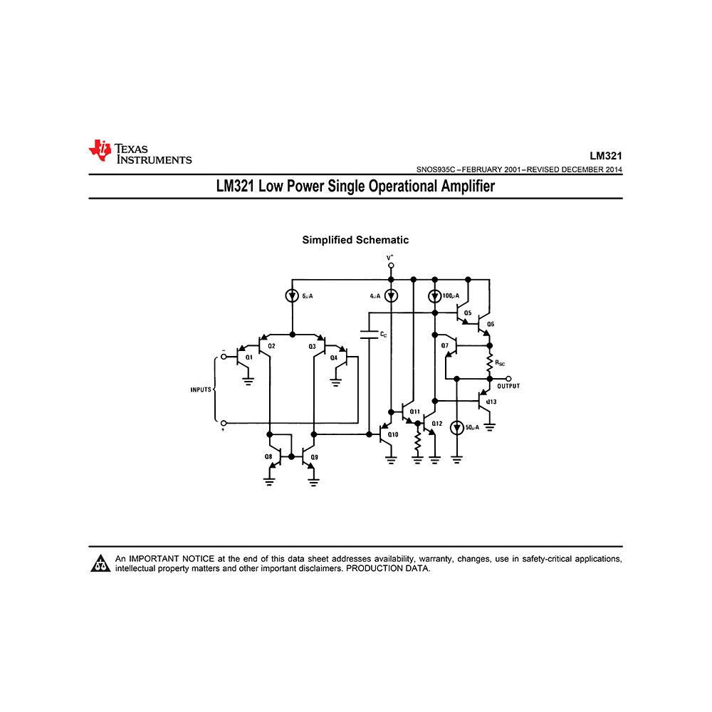
– Simplified Schematic
– Revision History
– Pin Configuration and Functions
– Pinout
– Specifications
– Maximum Differential Input Voltage
– Maximum Input Current
– Maximum Supply Voltage
– Maximum Input Voltage
– Maximum Output Short Circuit to GND
– Maximum Junction Temperature
– Maximum Mounting Temperature
– Maximum Storage temperature
– ESD Ratings
– Recommended Operating Conditions
– Thermal Information
– Electrical Characteristics
– Typical Characteristics
Figure 1. Small Signal Pulse Response
Figure 2. Large Signal Pulse Response
Figure 3. Supply Current vs. Supply Voltage
Figure 4. Sinking Current vs Output Voltage
Figure 5. Source Current vs. Output Voltage
Figure 6. Open Loop Frequency Response
– Detailed Description: Functional Block Diagram. Feature Description. Device Functional Modes. Common-Mode Voltage Range.
– Application and Implementation
– Typical Applications: Noninverting DC Gain Schematic. DC Summing Amplifier Schematic. Power Amplifier Schematic. LED Driver Schematic. Fixed Current Sources Schematic. Lamp Driver.
– Power Supply Recommendations
– Layout Guidelines. PCB Layout Example.
– Packaging Information
Why download the Datasheet?
This datasheet provides all the information from Texas Instruments about the LM321 operational amplifier, as detailed in the table of contents. Reading it completely will address most questions you might have. You can download and save it for offline use, including viewing it on your device or printing it for your convenience if you prefer a paper version.
How to download the Datasheet?
Download it by clicking the button below
Helped you out?
Glad to hear that. It would be awesome if you could . . .


