IRF540NS International Rectifier 100V 33A Power MOSFET Data Sheet
Download PDF datasheet for International Rectifier IRF540NS 100V 33A HEXFET D2PAC Power MOSFET (EN) 10 pages PD-91342 2002 zip
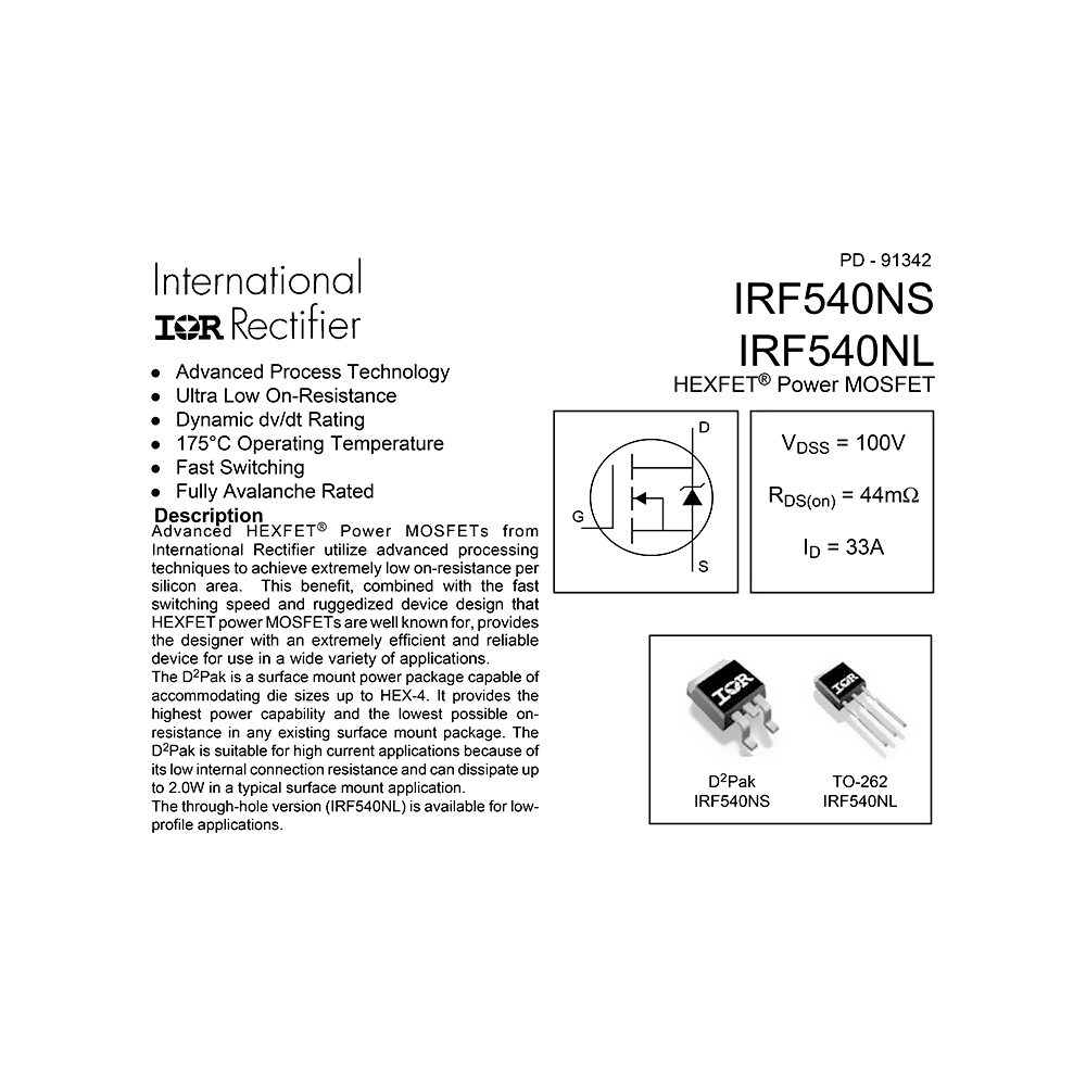
Description
This PDF datasheet is for the International Rectifier IRF540NS Power MOSFET.
About the Item
International Rectifier IRF540NS 100V 33A HEXFET D2PAC Power MOSFET
BRIEF DESCRIPTION
– Advanced Process Technology
– Ultra Low On-Resistance
– Dynamic dv/dt Rating
– 175 deg C Operating Temperature
– Fast Switching
– Fully Avalanche Rated
Advanced HEXFET Power MOSFETs from International Rectifier utilize advanced processing techniques to achieve extremely low on-resistance per silicon area. This benefit, combined with the fast switching speed and ruggedized device design that HEXFET power MOSFETs are well known for, provides the designer with an extremely efficient and reliable device for use in a wide variety of applications.
The D2Pak is a surface mount power package capable of accommodating die sizes up to HEX-4. It provides the highest power capability and the lowest possible onresistance in any existing surface mount package. The D2Pak is suitable for high current applications because of its low internal connection resistance and can dissipate up to 2.0W in a typical surface mount application.
Document(s) available
(PDF) DATASHEET
Available languages
ENGLISH (EN)
SUMMARY OF CONTENTS
– Absolute Maximum Ratings
– Internal Schematic Diagram
– IRF540NS pinout
– Thermal Resistance
– Electrical Characteristics
– Source-Drain Ratings and Characteristics
Fig 1. Typical Output Characteristics
Fig 3. Typical Transfer Characteristics
Fig 4. Normalized On-Resistance Vs. Temperature
Fig 5. Typical Capacitance Vs. Drain-to-Source Voltage
Fig 6. Typical Gate Charge Vs. Gate-to-Source Voltage
Fig 7. Typical Source-Drain Diode Forward Voltage
Fig 8. Maximum Safe Operating Area
Fig 9. Maximum Drain Current Vs. Case Temperature
Fig 10a. Switching Time Test Circuit
Fig 10b. Switching Time Waveforms
Fig 11. Maximum Effective Transient Thermal Impedance, Junction-to-Case
Fig 12a. Unclamped Inductive Test Circuit
Fig 12b. Unclamped Inductive Waveforms
Fig 12c. Maximum Avalanche Energy Vs. Drain Current
Fig 13a. Basic Gate Charge Waveform
Fig 13b. Gate Charge Test Circuit
– Peak Diode Recovery dv/dt Test Circuit
Fig 14. For N-channel HEXFET power MOSFETs
– Package Outline
Why download the Datasheet?
This datasheet provides all the information from INTERNATIONAL RECTIFIER about the IRF540NS transistor, as detailed in the table of contents. Reading it completely will address most questions you might have. You can download and save it for offline use, including viewing it on your device or printing it for your convenience if you prefer a paper version.
How to download the Datasheet?
Download it by clicking the button below
Helped you out?
Glad to hear that. It would be awesome if you could . . .


