H11A2 Fairchild Phototransistor Optocoupler Data Sheet
Download PDF datasheet for Fairchild Semiconductor H11A2 General Purpose 6-Pin Phototransistor Optocoupler (EN) 15 pages 2003 zip
Description
This PDF datasheet is for the Fairchild Semiconductor H11A2 phototransistor optocoupler.
About the Item
Fairchild Semiconductor H11A2 General Purpose 6-Pin Phototransistor Optocoupler
(PDF) DATASHEET (ENGLISH)
SUMMARY OF CONTENTS
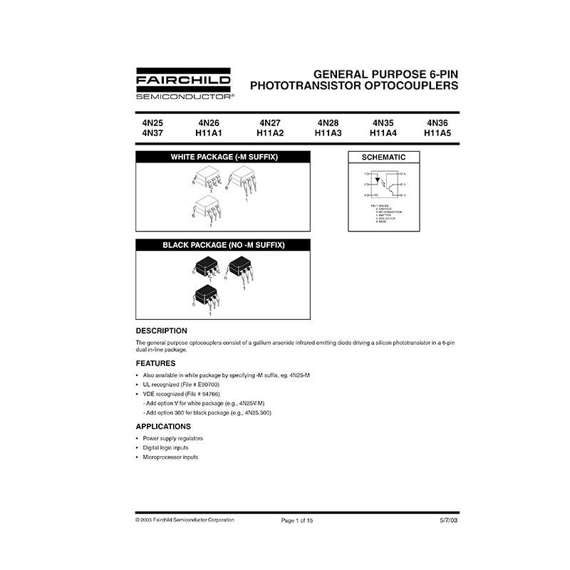
SCHEMATIC
PINOUT
DESCRIPTION
The general purpose optocouplers consist of a gallium arsenide infrared emitting diode driving a silicon phototransistor in a 6-pin dual in-line package.
FEATURES
– Also available in white package by specifying -M suffix
– UL recognized (File # E90700)
– VDE recognized (File # 94766)
APPLICATIONS
– Power supply regulators
– Digital logic inputs
– Microprocessor inputs
ABSOLUTE MAXIMUM RATINGS
ELECTRICAL CHARACTERISTICS
INDIVIDUAL COMPONENT CHARACTERISTICS
ISOLATION CHARACTERISTICS
TRANSFER CHARACTERISTICS
TYPICAL PERFORMANCE CURVES
Fig.1 LED Forward Voltage vs. Forward Current (Black Package)
Fig.2 LED Forward Voltage vs. Forward Current (White Package)
Fig.3 Normalized CTR vs. Forward Current (Black Package)
Fig.4 Normalized CTR vs. Forward Current (White Package)
Fig.5 Normalized CTR vs. Ambient Temperature (Black Package)
Fig.6 Normalized CTR vs. Ambient Temperature (White Package)
Fig.7 CTR vs. RBE (Unsaturated) (Black Package)
Fig.8 CTR vs. RBE (Unsaturated) (White Package)
Fig.9 CTR vs. RBE (Saturated) (Black Package)
Fig.10 CTR vs. RBE (Saturated) (White Package)
Fig.11 Collector-Emitter Saturation Voltage vs Collector Current (Black Package)
Fig.12 Collector-Emitter Saturation Voltage vs Collector Current (White Package)
Fig.13 Switching Speed vs. Load Resistor (Black Package)
Fig.14 Switching Speed vs. Load Resistor (White Package)
Fig.15 Normalized ton vs. RBE (Black Package)
Fig.16 Normalized ton vs. RBE (White Package)
Fig.17 Normalized toff vs. RBE (Black Package)
Fig.18 Normalized toff vs. RBE (White Package)
Fig.19 Dark Current vs. Ambient Temperature
Fig.20. Switching Time Test Circuit and Waveforms
PACKAGE DIMENSIONS (THROUGH HOLE)
PACKAGE DIMENSIONS (0.4″ LEAD SPACING)
PACKAGE DIMENSIONS (SURFACE MOUNT)
RECOMMENDED PAD LAYOUT FOR SURFACE MOUNT LEADFORM
ORDERING INFORMATION
MARKING INFORMATION
REFLOW PROFILE
Why download the Datasheet?
This datasheet provides all the information from Fairchild Semiconductor about the H11A2 Phototransistor Optocoupler, as detailed in the table of contents. Reading it completely will address most questions you might have. You can download and save it for offline use, including viewing it on your device or printing it for your convenience if you prefer a paper version.
How to download the Datasheet?
Download it by clicking the button below
Helped you out?
Glad to hear that. It would be awesome if you could . . .


